Professional designer and manufacture of CCD machines for ONE STOP SOLUTION.
Language
Professional designer and manufacture of CCD machines for ONE STOP SOLUTION.
"Precise Positioning, Consistent Thickness" Screen Printing Technology for Semiconductor Wafer Coating Glass Powder Processes
A wafer is a silicon chip used in the production of silicon semiconductor integrated circuits, and its original material is silicon. High purity polycrystalline silicon is dissolved and doped into silicon crystal seed, then slowly pulled out to form cylindrical single-crystal silicon. Silicon crystal rods are ground, polished, and sliced to form silicon wafers, also known as wafers.
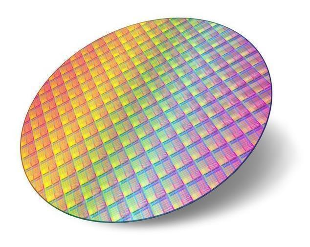
Silicon wafers can be processed and manufactured into a variety of circuit element structures, which become integrated circuits with specific electrical functions. In producing electronic components from wafers, it is necessary to coat the wafers with glass powder to ensure that a protective glass layer can be formed on the side of the chip after cutting.
Currently, most of the glass powder coated on the wafer is carried out manually, manually mixing the glass powder with water, and then brushing the mixed glass powder onto the wafer. This method of painting not only has a lower speed, but also affects the production speed of the product, and the production cost of the product will also increase. Moreover, the quality of the glass powder coating depends on the labour ability of the workers, and the stability of the coating is poor, which easily leads to the residual glass remaining on the wafer surface. This leads to a low qualification rate of electronic components and further increases the production cost of the product. Although there are also related production processes to improve the quality of coating by wiping powder or filling equipment, but still can not be a good solution to improve the batch coating speed, consistency of the printed parts and thickness, operation is cumbersome and complex and so on a variety of issues.
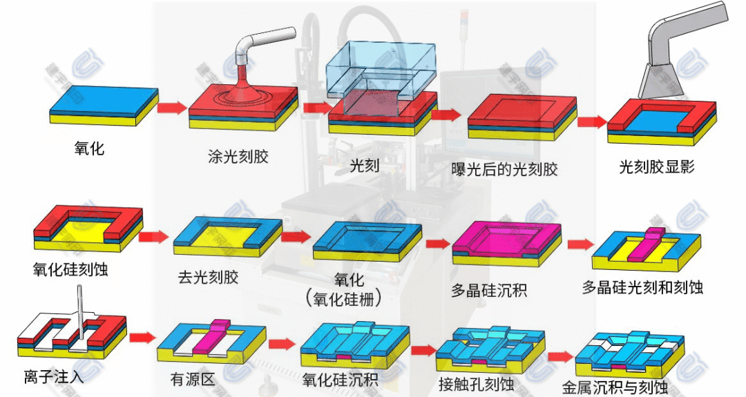
Wafer processing process diagram
Thick film screen printing technology has a wide range of applications in semiconductor production, which can be applied to wafer coating glass powder, photoresist, semiconductor packaging link solder printing and passivation of insulating film and other semiconductor production processes. The high-precision screen printing machine developed and produced by Jianyu Screen Printing has been highly recognized and trusted by customers in the semiconductor production field due to its high printing precision, uniform thickness, high degree of automation and easy operation.
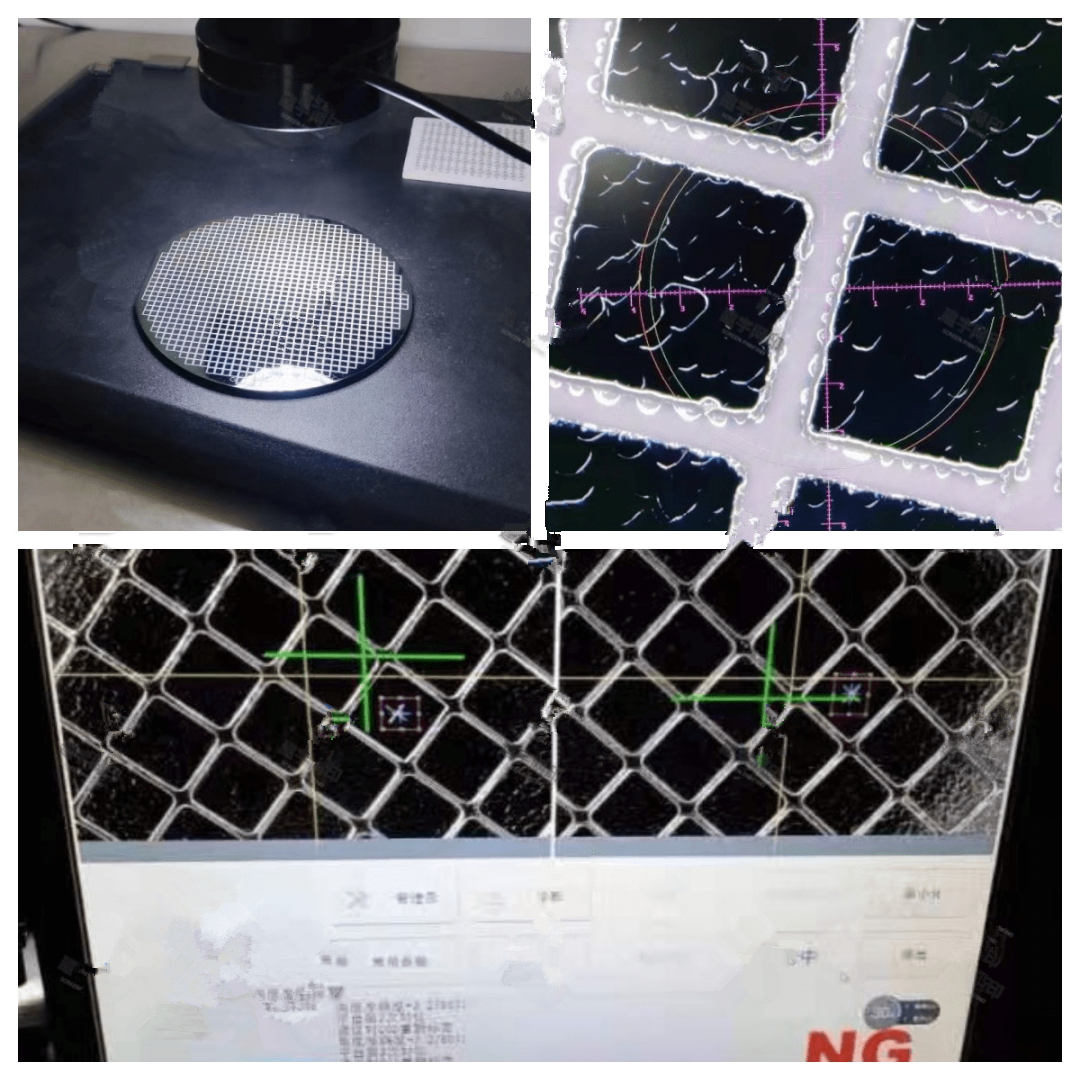
Vility high-precision screen printing machine in the wafer glass powder coating process.
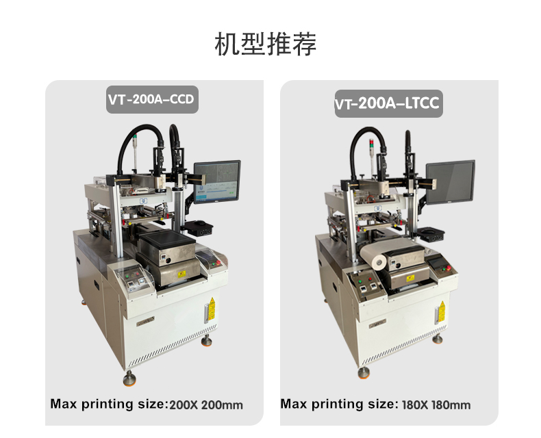
Equipment features:
1, CCD automatic visual alignment system can quickly find the mark point, and within 0.3 seconds quickly identify the product substrate placement deviation and automatic visual correction, simple and convenient operation, printing alignment accuracy ± 5um.
2、Printing stroke using servo-driven and high-precision imported linear guide, so that the scraping knife maintains uniform speed and stable state, after the overall debugging and calibration of the system, to effectively ensure the uniform consistency of the printed coating, the ink layer thickness deviation accuracy of up to ± 4um.
3、The printing table adopts servo drive system, which has excellent stability and labour resistance—full digital positioning, high printing efficiency, buffer graphics overprint precision.
Domestic semiconductor key components development speed continues to increase, and the production of these components more and more need high precision screen printing machine to improve production efficiency and product stability, Jianyu Screen Printing will always adhere to the "technology is king, innovation-based" business philosophy, to increase R & D and innovation, for the domestic semiconductor production field to provide faster, stronger and more comprehensive screen printing technology services for the domestic semiconductor production field.

VILITY is a Professional manufacturer, providing ONE-STOP SOLUTION for intelligent printing industry.